Understanding Energy Bands and Semiconductor Physics
Explore the fundamental concepts of energy bands in solids, including valence bands, conduction bands, and the forbidden energy gap. Learn about intrinsic and extrinsic semiconductors, doping, and the behavior of charge carriers like electrons and holes. This guide also touches upon generation, recombination, and poten
In the study of solid-state physics, the ability of a material to conduct electricity is not a random property but is fundamentally determined by the arrangement of its electrons within specific energy levels. When atoms come together to form a solid, their discrete energy levels merge into continuous ranges known as energy bands. Understanding these bands is the key to distinguishing between metals, insulators, and the versatile world of semiconductors.
Energy Bands in Solids
The electronic structure of a solid is characterized by three primary components: the valence band, the conduction band, and the forbidden energy gap.
The Valence Energy Band (VB)
The valence band is the highest energy band that is occupied by valence electrons. At absolute zero temperature, this band is completely filled with electrons. Because the electrons are "trapped" in these bonds, they are not capable of gaining energy from an external electric field to move freely through the crystal.
The Conduction Energy Band (CB)
The conduction band represents the range of minimum energy where electrons can move freely to contribute to an electric current. This band can be empty or partially filled. Electrons reach this band by breaking their covalent bonds, gaining enough energy to jump from the valence band.
The Forbidden Energy Gap (ΔEg)
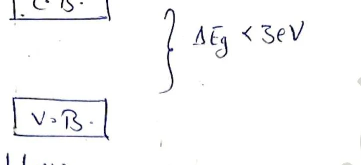
The region between the top of the valence band (Ev) and the bottom of the conduction band (Ec) is known as the forbidden energy gap, or band gap. No electrons can exist within this gap. The magnitude of this gap determines the electrical classification of the material:
ΔEg=Ec−Ev
Diagram showing the conduction band (C.B.) and valence band (V.B.) with a band gap energy (ΔEg) less than 3 eV.
Conductors: Have a very small or zero energy gap (ΔEg≃0), allowing electrons to flow easily.
Insulators: Possess a very large forbidden gap (typically >3 eV), making it nearly impossible for electrons to jump to the conduction band.
Semiconductors: Have a small energy gap (e.g., Silicon ≈1.1 eV, Germanium ≈0.7 eV).
Exam Tip: Semiconductors exhibit a unique temperature relationship. Unlike metals, as temperature increases, their conductivity increases and their resistivity decreases because thermal energy helps electrons jump the small gap.
Types of Semiconductors
Semiconductors are categorized based on their purity and how they are manipulated to conduct electricity.
Intrinsic Semiconductors
An intrinsic semiconductor is a pure form of the material (such as pure Silicon or Germanium). In these materials, the number of free electrons (ne) is exactly equal to the number of holes (nh) created by thermal excitation:
ne=nh
Because the number of charge carriers is relatively low at room temperature, intrinsic semiconductors have limited practical use in electronic devices.
Extrinsic Semiconductors and Doping
To make semiconductors useful, we perform doping—the process of adding specific impurities to the crystal lattice to increase the number of charge carriers. This results in extrinsic semiconductors.
n-type Semiconductors
n-type semiconductors are created by adding Group V elements (such as Phosphorus (P), Arsenic (As), or Antimony (Sb)) to a Group IV element like Silicon. Since Group V atoms have five valence electrons and only four are needed for bonding, one extra electron is provided. These impurities are called donors. In n-type material, electrons are the majority carriers (ne>nh).
This is a Lewis structure diagram illustrating the bonding between a phosphorus atom and silicon atoms, with some electrons shown as dots and circles.
p-type Semiconductors
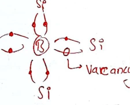
p-type semiconductors are created by adding Group III elements (such as Boron (B), Aluminum (Al), or Gallium (Ga)) to a Group IV element. These atoms have only three valence electrons, creating a deficiency or "vacancy" in the covalent bond. This vacancy is called a hole, and the impurities are known as acceptors. In p-type material, holes are the majority carriers (nh>ne).
A diagram illustrating a Boron atom (B) bonded to Silicon atoms (Si), with a vacancy indicated.
Charge Carriers and Conductivity
Holes and Electrical Current
In semiconductor physics, a hole is treated as a physical particle with a positive charge. It is essentially the absence of an electron in a covalent bond. When an electric field is applied, holes move in the direction opposite to the flow of electrons. The total electrical current (I) in a semiconductor is the sum of the electron current (Ie) and the hole current (Ih):
I=Ie+Ih
Generation and Recombination
The concentration of these carriers is dynamic. Due to thermal effects, electrons can jump from the valence band to the conduction band, creating an electron-hole pair; this is called generation. Conversely, when an electron falls back into a hole, the pair is annihilated; this is called recombination.
The relationship between the concentration of electrons and holes in equilibrium is governed by the Law of Mass Action, which relates them to the intrinsic carrier concentration (ni):
ne⋅nh=ni2
Diffusion and Potential Barriers
When there is a concentration gradient (a difference in carrier density between two regions), carriers will naturally move from the high-concentration area to the low-concentration area. This movement is called diffusion.
In a p-n junction, the diffusion of electrons from the n-side to the p-side and holes from the p-side to the n-side creates a depletion layer of ions. This layer generates an internal electric field that creates a potential barrier, which opposes further diffusion. For Silicon, this barrier (knee voltage) is approximately 0.7 V, while for Germanium, it is approximately 0.3 V.
Keep reading for free.
Create an account to finish this reading and make it part of your study routine.